Q: What's the difference between Ka7500 and TL494?
A: These two ICs have the same function, the pin function is exactly the same, only the name is different, they can be completely replaced
The above question about what is the difference between Ka7500 and TL494 is often asked, but in fact the two are the same. In this article, our team will focus on TL494 in detail, let's get starting.
The TL494, a switching power supply pulse width modulation (PWM) controller chip designed and introduced by Texas Instruments in the early 1980s, has two complete pulse width modulation control circuits. TL494 has become an industry standard chip, produced by many IC manufacturers. It has also been named other models, such as Fairchild named its TL494-compatible chip KA7500.
Modulation mode: fixed frequency modulation width
Control mode: voltage mode
Maximum rated frequency: 300000Hz
Output port: double-ended interleaved
Maximum duty cycle per end: 45%
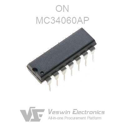
Package: SOP-16, DIP-16
Common topologies: Buck, Push-Pull, Half Bridge
5V reference source
The TL494 has a built-in reference source that based on the bandgap principle. The stable output voltage of the reference source is 5V, provided that the VCC voltage is above 7V and the error is within 100mV. The output pin of the reference source is pin 14 REF.
Ramp oscillator
The TL494 has a built-in linear sawtooth oscillator that generates a sawtooth waveform from 0.3 to 3V. The oscillation frequency can be adjusted by an external resistor Rt and a capacitor Ct. The oscillation frequency is: f=1/RtCt, where Rt is in ohms and Ct is in farads. The sawtooth wave can be measured at the Ct pin.
Operational Amplifier
The TL494 incorporates two operational amplifiers powered from a single supply. The op-amp transfer function is ft(ni,inv)=A(ni-inv), but cannot cross out the output swing. In general power supply circuits, op amps are connected to closed-loop operation. In a few special cases, open loop is used, and the signal is input from outside. A diode is connected to the output of each of the two op-amps, which is connected to the COMP pin and the back-end circuit (comparator). This ensures that the higher output of the two op-amps goes to the post-stage circuit.
Comparator
The signal from the op-amp output (COMP pin) enters the positive input of the comparator inside the chip and is compared with the sawtooth wave that enters the negative input. When the sawtooth waveform is higher than the signal at the COMP pin, the comparator outputs 0, and vice versa, it outputs 1.
Pulse Trigger
The pulse trigger turns on at the falling edge of the sawtooth wave and the comparator output is 1, causing one of the two outputs (in turn) to turn on the on-chip triode and turn off when the comparator output drops to 0.
Quiet Zone Time Comparator
The dead time is set by Dead Time Control pin 4, which limits the maximum duty cycle by interfering with the pulse flip-flop through a comparator. The maximum duty cycle per end can be set to 45%, and the maximum duty cycle is about 42% at operating frequencies above 150KHz. (When the DTC pin level is set to 0).
The pin functions of the TL494 are as follows:
1, pin 16 and 2, pin 15 are the in-phase input and reverse input of error amplifier 1 and error amplifier 2 respectively; pin 3 is the feedback input; pin 4 is the dead time control; pins 5 and 6 are connected to the timing capacitor and resistor of the RC oscillator; pin 7 is grounded; pins 8, 9, 11 and 10 are the collector and emitter of the two internal drive transistors respectively. Pin 12 is the positive side of the power supply; pin 13 is the output state control terminal, when pin 13 is high, the two internal drive transistors alternately on, when pin 13 is low, the two internal drive transistors simultaneously on or off, at this time can only control a switch tube. Pin 14 is the internal 5V reference voltage output of the IC.
1. Circuit diagram of a step-down switching regulator composed of TL494.
2. A very typical TL494 computer switching power supply circuit diagram
Switching mode power supply is a high-frequency power conversion device that converts a bit of voltage to the voltage or current required by the user through a different form of architecture, also known as a switching power supply or switching converter. It is characterized by small size, light weight and high efficiency.
Switching power supply products are widely used in industrial automation control, military equipment, scientific research equipment, LED lighting, industrial control equipment, communication equipment, electric power equipment, instruments, medical equipment, semiconductor refrigeration and heating, air purifiers, electronic refrigerators, LCD monitors, LED lamps and lanterns, communication equipment, audio-visual products, security monitoring, LED lighting, computer cases, digital products and instruments, etc.
Inverter is a converter that converts DC power (battery, storage battery) into constant frequency and voltage or FM AC power (generally 220V, 50Hz sine wave). It includes an inverter bridge, control logic and filter circuit.
Simply put, the inverter, in combination with the control device, can bring energy saving effect, so the application area is expanding. It is widely used in air conditioners, home theaters, electric sanders, power tools, sewing machines, DVDs, VCDs, computers, TVs, washing machines, range hoods, refrigerators, VCRs, massagers, fans, lighting, etc.
In order to significantly reduce the cost and power consumption of the system, PWM controllers control analog circuits digitally, and many microcontrollers contain PWM controllers within them. The main features are:
3.3V/5V/12V overvoltage protection
3.3V/±5V/±12V undervoltage protection
Over power protection
Short circuit protection
AC input undervoltage protection
PG circuit
Remote power-up signal
Power-up signal and PG signal delay
Two bypass regulators TL431 to stabilize 3.3V and 5V independent power supplies
Soft start and maximum 93% duty cycle
Hot News
