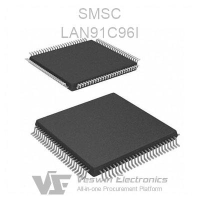
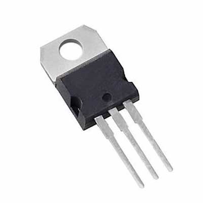
CD4066 is an integrated circuit that belongs to the CMOS family of four-channel bidirectional analog switches. It is a common electronic component widely used in multiplexing and signal switching applications of analog or digital signals. There are 4 independent analog switches inside each package of CD4066, and each analog switch has three terminals of input, output and control, and the input and output terminals are interchangeable. It allows multiple input signals to be transmitted to one output signal by selecting one or more channels, or an input signal from one signal source to be transmitted to different output channels. This is useful for implementing signal switching, signal routing, multiplexing, etc.
Catalog:
CD4066 Functional block diagram
What is the difference between CD4016 and CD4066?
To obtain the CD4066 datasheet, you should download the datasheet from a reliable source. Veswin is a reputable electronic components distributor, to ensure that you have the most accurate and up-to-date information. You can download the CD4066 datasheet from Veswin.
The sixteen-sound sound circuit is composed of another analog sound circuit KD9561. According to the internal curing program of its circuit, KD9561 contains 4 kinds of analog sound effects, namely the sound of machine gun, police siren, ambulance and fire engine. It has two sounding trigger terminals SELl and SEL2, which can be triggered by high and low levels or floating them.
If you change the resistance value of its oscillating resistor and use different trigger levels for the two trigger terminals, through combined transformation, you can form a sounding circuit that can emit 16 kinds of sounds. The circuit composition is shown in the figure.
In the self-locking touch switch circuit composed of CD4066B, when the touch switch S1 is activated, R4 is driven high, and the control voltage becomes high, which will latch the switch. When S2 is activated, R4 goes low and the control voltage goes low, which deactivates the switch.
The CD4066 is a 14-pin IC, and its pin configuration is as follows:
CD4068
HEF4066
CD4066 is a quad bidirectional analog switch, mainly used for multiplexing of analog or digital signals. There are 4 independent analog switches inside each package of CD4066, and each analog switch has three terminals of input, output and control, and the input and output terminals are interchangeable.
When the control terminal is high, the switch is turned on; when the control terminal is low, the switch is off. When the analog switch is turned on, the on-resistance is tens of ohms; when the analog switch is turned off, it presents a high impedance, which can be regarded as an open circuit.
The analog switch can transmit digital signal and analog signal, and the upper limit frequency of the analog signal that can be transmitted is 40MHz. Crosstalk between switches is minimal, typically -50dB. The terminal arrangement of CD4066 is the same as that of CD4016, but it has relatively low on-resistance.
In addition, the on-resistance is essentially constant over the entire input signal range. CD4066 is composed of four mutually independent bidirectional switches, each switch has a control signal, and the p and n devices in the switch switch simultaneously under the action of the control signal.
4-Input Multiplexer
Signal Level Shifting
Sample and Hold circuits
Network switching
Communication Systems
Dead band filter
Battery-Powered Devices
Industrial Control Systems
Squelch control
CMOS logic implementation
Audio Signal Switching
Signal Routing and Patching
Data Routing
Signal Isolation
Analog and Digital Signal Multiplexing
Sogic Implementation of Transmission-Gates
Digital control of phase impedance, frequency and analog-signal gain
The CD4066 has a very low internal resistance of only 5Ω, while the CD4016 IC has an on-state resistance of 200Ω. Therefore, CD4066 is suitable for places with weak signals or places where higher switching efficiency is required.
Also, the CD4066 is primarily designed for analog signal applications, while the CD4016 is designed for digital signal switching tasks.
Hot News


