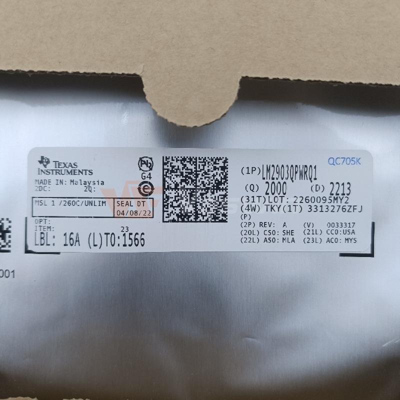
Many smt processing manufacturers, in addition to fixing components in the solder joints of electronic product printed circuit boards, must be able to pass a certain amount of current stably and reliably. The quality of welding directly affects the quality of electronic products. So what are the environmental related welding defects?
bubble
In the process of smt processing and soldering, the lead of the soldered component is inserted into the socket of the printed circuit board. After soldering, there is a squirting solder bump at the root of the lead, and there is a small hole in the center, and the bottom of the hole may be covered. A large void, this weld defect is called a bubble. The reason for the occurrence of the void is that the heat capacity of the copper foil side of the printed circuit board is large, and although the soldering has ended, its back surface has not cooled. Due to the thermal inertia, the temperature is still rising, and the outside of the solder joint begins to solidify, and the gas generated inside the solder joint is discharged, causing a void. In addition, stains on the pads, poor oxidation of component leads, too large via holes, too thin component leads, too little solder, and too much rosin can cause this phenomenon.

Insufficient solder
When soldering with an electric soldering iron, when the solder is too small, the wetting is poor, and the solder cannot form a smooth surface into a flat mat. This soldering defect is called insufficient solder. One of the reasons for this defect is that the wire is removed too early; the second is that the effective area of the soldering iron in contact with the solder is small, the temperature is too high or the welding time is too long. Insufficient soldering material This soldering defect may cause poor conduction of the circuit due to environmental degradation. The hazard of this soldering defect is that the mechanical strength between the solder joints is insufficient and can be re-welded by adding solder wire.
overheat
This soldering defect is characterized by white solder joints, no metallic luster, and a rough surface. The main reason for the overheating is that the power of the soldering iron is too large, the temperature of the soldering iron is too high, and the heating time is too long. The hazard of overheating is that the pad is easily peeled off, which easily causes a decrease in mechanical strength between the solder joints.
Cold welding
In the process of smt processing and welding, the brazing material has not completely solidified, and the wire or lead of the welded component is moved. At this time, the surface of the soldering point is dull and dull, the structure is loose, and there are fine cracks. This welding defect is called cold welding. The reason for the cold welding is that the wire or lead of the soldered component is removed too early, the soldered component is shaken, and the power of the soldering iron is insufficient. The hazard of cold welding is that the joint strength between the solder joints is low and the conductivity is not good. The measure to prevent cold welding is to avoid the jitter of the wires or leads of the soldered components during the soldering process. If in doubt, refill the needle if necessary.
Copper foil lifting, peeling, and peeling off
The copper foil is lifted and peeled off from the printed circuit board, and is severely or completely broken. This phenomenon is called copper foil lifting and peeling. The reason why the copper foil is lifted and peeled off is that when the manual welding is performed, the operation method is not grasped, and a part of the circuit is superheated or concentrated in the heating circuit; or the soldering iron is used for soldering. The hazard of copper foil lifting and peeling is a short circuit in the circuit. The measures to solve the problem of lifting, peeling and peeling off the copper foil are to strengthen the training, practice repeatedly, and master the welding essentials.
Pinhole
The reason for the pinhole is mainly caused by the too large gap between the pad hole and the lead. The hazard of the pinhole is that the joint strength of the solder joint is low and the solder joint is easily corroded. The measures to solve the pinhole are caused by the printed circuit board, and the pad hole opened should not be too large.
Rosin welding
A layer of flux film and dissolved oxide or contaminant is formed between the needle material and the lead of the component to be welded to form a solder joint in the shape of bean curd. This phenomenon is called rosin welding, and the cause of the rosin welding is the soldering iron tip. Remove too early so that the flux does not float to the surface. The hazard of rosin welding is that the connection strength between the solder joints is insufficient, and the circuit conduction failure may occur when the connection is broken. The measures to prevent rosin welding are not to add too much flux, and the welding time should be appropriate.
Hot News