Today, the world's largest integrated circuit (Integrated Circuit, IC, Taiwan called fab) is mainly concentrated in a few developed countries and regions such as the United States, Japan, Western Europe, Singapore and Taiwan, of which Taiwan has a pivotal position. However, due to the impact of a series of events such as earthquakes, financial crises, and government changes in Taiwan in recent years, the island of Taiwan, which has a shortage of resources, a small market, and a floating population, has become more turbulent, which has led to a fab move. The trend. The mainland of China, which has the advantages of vast territory, abundant resources, huge potential market, and abundant human resources supply, has naturally become its preferred place of relocation.
The products produced by the fab actually include two parts: wafer slicing (also referred to as wafer) and VLSI chip (referred to as chip). The former is just a smooth circular sheet like a mirror. In a strict sense, it has no practical application value, but is a raw material for deep processing of the subsequent chip production process. The latter is the ultimate product that should be directly applied in many industries such as computers, electronics, communications, etc. It can include CPUs, memory units and other professional application chips.
A Very Large Scale Integration Circuit (VLSI) is an integrated circuit that combines a large number of transistors into a single chip, which is more integrated than a large-scale integrated circuit. The number of integrated transistors varies among different standards. Since the 1970s, with the development of complex semiconductors and communication technologies, the research and development of integrated circuits has gradually begun. The control core microprocessor in the computer is the most typical example of VLSI. VLSI design, especially digital integrated circuit, is usually carried out by electronic design automation, and has become an important branch of computer engineering. one.
The so-called wafer is actually the single crystal silicon that China used to call. In the 1960s and 1970s, China has developed monocrystalline silicon and was listed as one of the ten days of news of the year. However, due to its numerous integrated circuit manufacturing processes (more than 400 processes from raw material melting to final product packaging), the process is complex and the technical difficulty is very high. In the years after, China has been able to fully grasp its series of key technologies. Therefore, it is only possible to produce some of its products on a small scale, and it cannot form economies of scale. There is a huge gap in quality and quantity compared with some developed countries and regions that have formed a complete wafer manufacturing industry.
In a big way, wafer production involves two major steps: ingot fabrication and wafer fabrication. It can be subdivided into the following main processes (where the ingot fabrication includes only the first process below, and the rest are all Wafer manufacturing, so sometimes they are collectively referred to as crystal column post-processing steps):
Polycrystalline silicon - single crystal silicon - crystal rod growth - ingot cutting and inspection - outer diameter grinding - slicing - round edge - surface grinding - etching - deuterium - polishing - (evolution - Etching - go to 疵) - cleaning - inspection - packaging
1. Ingot growth process
It can be subdivided into: 1) Melt Down: The block-shaped high-purity polycrystalline silicon is placed in a quartz crucible and heated to a melting point of 1420 ° C or more to completely melt. 2) Neck Growth: After the temperature of the silicon melt is stabilized, the seed crystal in the direction of <1.0.0> is slowly inserted into it, and then the seed crystal is slowly lifted upward to make the diameter smaller. To a certain size (generally about 6mm), maintain this true path and stretch 100---200mm to eliminate the difference in grain alignment between the seeds. 3), Crown Growth: After the neck is completed, slowly reduce the lifting speed and temperature, and gradually increase the neck diameter to the required size (such as 5, 6, 8, 12, etc.). 4), Body Growth: Constantly adjust the lifting speed and melting temperature to maintain a fixed ingot diameter, only until the length of the ingot reaches a predetermined value. 5) Tail Growth: When the length of the ingot reaches a predetermined value, the lifting speed is gradually increased and the melting temperature is increased, so that the diameter of the ingot is gradually reduced to avoid the phenomenon of displacement and slip due to thermal stress. Produced, eventually completely separating the ingot from the liquid surface. A complete ingot is obtained.
2, crystal rod cutting and testing (CutTIng & InspecTIon)
the length of the ingot is removed from the head and tail portion of the smaller diameter, and the size is tested to determine the process parameters of the next step.
3. Surface Grinding & Shaping
Due to the deviation of the outer diameter and the roundness of the ingot during the growth process of the ingot, the outer cylindrical surface is also uneven, so the outer diameter must be trimmed and ground. Make the size and shape error less than the allowable deviation.
4. Wire Saw Slicing
Due to the very high hardness of silicon, in this sequence, a thin blade with a ring-shaped diamond particle embedded in its inner diameter edge is used to cut the ingot into a sheet.
5. Edge profiling
Since the outer edge of the wafer that has just been cut is very sharp, the single crystal silicon is a brittle material. In order to avoid the cracking of the wafer, the strength of the wafer is damaged, the surface of the wafer is damaged, and the particles are contaminated in the subsequent process. The edge and outer diameter dimensions of the wafer must be automatically trimmed with a dedicated computer control device.
6. Lapping
The purpose of grinding is to remove the saw marks and breakage on the surface of the wafer during cutting to achieve the desired finish of the wafer surface.
7. Etching
A chemical etching method is used to remove a damaged layer on the surface of the wafer due to processing pressure after processing in the previous processes.
8. Gettering
Use sandblasting to drive the defects and defects on the wafer to the lower half to facilitate subsequent processing.
9. Polishing
Polishing the edges and surfaces of the wafer, further removing the particles attached to the wafer, and obtaining excellent surface flatness for the wafer processing to be described later. Process processing.
10. Cleaning
The finished wafer is thoroughly cleaned and air dried.
11. Inspection (IinspecTIon)
Perform the final comprehensive inspection to ensure that the product finally meets the specified specifications such as size, shape, surface finish and flatness.
12. Packing
The products are separated, packaged and boxed with flexible materials, ready to be sent to the chip manufacturing workshop or sent to the ordering customer.
The manufacturing process of the chip can be divided into several steps, such as a wafer processing process (Wafer FabricaTIon), a wafer needle testing process (Wafer Probe), a packaging process, and an initial test and final test. The wafer processing step and the wafer needle measurement step are Front End processes, and the assembly process and the test process are Back End processes.
1. Wafer processing process
The main work of this process is to make circuits and electronic components (such as transistors, capacitors, logic switches, etc.) on the wafer.
The processing procedure is usually related to the type of product and the technology used, but the general basic procedure is to properly clean the wafer, then perform oxidation and chemical vapor deposition on the surface, and then apply film, exposure, development, etching, ion implantation. Repeated steps such as implantation, metal sputtering, etc., finally complete the processing of several layers of circuits and components on the wafer.
2. Wafer Needle Measurement Process
After the previous process, a small grid, ie, a die, is formed on the wafer. Under normal circumstances, in order to facilitate testing and improve efficiency, the same variety is produced on a wafer. , specifications of the product; but also can be produced according to the needs of several different varieties, specifications of the product. After measuring the electrical characteristics of each die with a probe, and marking the unqualified die, the wafer is cut and divided into individual grains, and then according to their electrical characteristics. Classification, loading into different trays, and rejecting unqualified grains.
3, the assembly process
is to fix a single die on the chip base of plastic or ceramic, and put some lead ends on the die and the bottom of the base
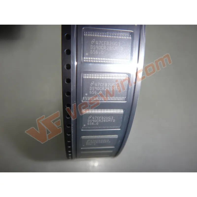
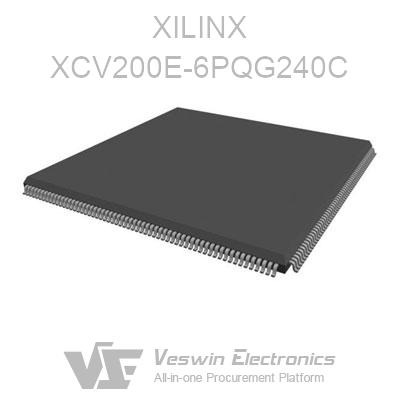
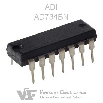
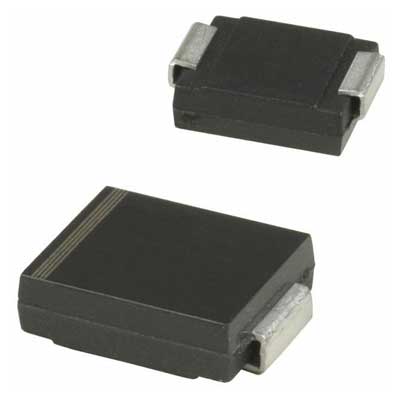
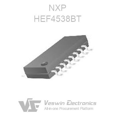
The protruding pins are connected for connection with the external circuit board, and finally the plastic cover is covered and sealed with glue. Its purpose is to protect the crystal grains from mechanical scratches or high temperature damage. At this point, we have made an integrated circuit chip (that is, those black or brown that we can see in the computer, rectangular blocks with many pins or leads on both sides or four sides).
4. Test procedure
The last process of chip manufacturing is test, which can be divided into general test and special test. The former is sealed after the test.
The chip is tested in various environments for electrical characteristics such as power consumption, operating speed, and withstand voltage. The tested chips are classified into different grades according to electrical characteristics. The special test is based on the technical parameters of the customer's special needs, taking some chips from similar parameter specifications and varieties, and doing targeted and specialized tests to see if they can meet the special needs of customers to decide whether they must design for customers. Dedicated chip. After the general test, the product is labeled with the specifications, model and date of manufacture, and packaged. The chip that passed the test is classified as a downgrade or waste according to the parameters it has reached.
Hot News
