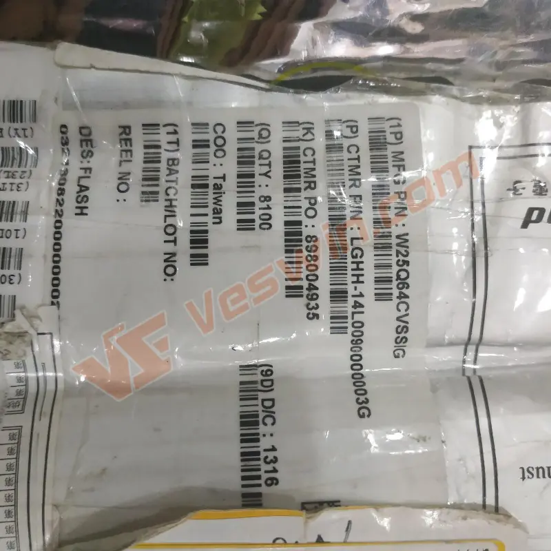
W25Q32 refers to a specific model of serial flash memory produced by Winbond Electronics Corporation. In particular, the "W25Q32" is part of the W25Q series, which consists of a range of flash memory chips differing in capacity and features.
Standard SPI Instructions:
The W25Q32JV is accessed through an SPI-compatible bus consisting of four signals: Serial Clock (CLK), Chip Select (/CS), Serial Data Input (DI), and Serial Data Output (DO). Standard SPI instructions use the DI
input pin to serially write instructions, addresses, or data to the device on the rising edge of CLK. The DO output pin reads data or status from the device on the falling edge of CLK. SPI bus operation Mode 0 (0,0) and 3 (1,1) are supported. The primary difference between Mode 0 and
Mode 3 concerns the normal state of the CLK signal when the SPI bus master is on standby and data is not being transferred to the Serial Flash. For Mode 0, the CLK signal is typically low on the falling and rising
edges of /CS. For Mode 3, the CLK signal is usually high on the falling and rising edges of /CS.
Dual SPI Instructions:
The W25Q32JV supports Dual SPI operation when using instructions such as "Fast Read Dual Output (3Bh)" and "Fast Read Dual I/O (BBh)". These instructions allow data to be transferred to or from the device
at two to three times the rate of ordinary Serial Flash devices. The Dual SPI Read instructions are ideal for quickly downloading code to RAM upon power-up (code-shadowing) or for executing non-speed-critical
code directly from the SPI bus (XIP). When using Dual SPI instructions, the DI and DO pins become bidirectional I/O pins: IO0 and IO1.

Quad SPI Instructions:
The W25Q32JV supports Quad SPI operation when using instructions such as "Fast Read Quad Output (6Bh)" and "Fast Read Quad I/O (EBh). These instructions allow data to be transferred to or from the device
four to six times the rate of ordinary Serial Flash. The Quad Read instructions offer a significant improvement in continuous and random access transfer rates, allowing fast code-shadowing to RAM or
execution directly from the SPI bus (XIP). When using Quad SPI instructions, the DI and DO pins become bidirectional IO0 and IO1, and the /WP and /HOLD pins become IO2 and IO3 respectively. Quad SPI
instructions require the non-volatile Quad Enable bit (QE) in Status Register-2 to be set.
Hold Function:
For Standard SPI and Dual SPI operations, the /HOLD signal allows the W25Q32JV operation to be paused while actively selected (when /CS is low). The /HOLD function may be helpful in cases where the SPI
data and clock signals are shared with other devices. For example, consider if the page buffer was only partially written when a priority interrupt requires using the SPI bus. In this case, the /HOLD function can
save the state of the instruction and the data in the buffer so programming can resume where it left off once the bus is available again. The /HOLD function is only available for standard SPI and Dual SPI operation, not during Quad SPI. The Quad Enable Bit QE in Status Register-2 determines if the pin is used as an a/HOLD pin or data I/O pin. When QE=0 (factory default), the pin is /HOLD; when QE=1, the pin will
become an I/O pin, /HOLD function is no longer available.
To initiate a /HOLD condition, the device must be selected with /CS low. A /HOLD condition will activate on the falling edge of the /HOLD signal if the CLK signal is already low. If the CLK is not already low, the /HOLD
condition will activate after the next falling edge of CLK. The /HOLD condition will terminate on the rising edge of the /HOLD signal if the CLK signal is already low. If the CLK is not already low, the /HOLD condition
will terminate after the next falling edge of CLK. During a /HOLD condition, the Serial Data Output (DO) is high impedance, and the Serial Data Input (DI) and Serial Clock (CLK) are ignored. The Chip Select (/CS)
signal should be kept active (low) for the whole duration of the /HOLD operation to avoid resetting the internal logic state of the device.
Various densities and packaging options: The W25Q32JV is available in multiple thicknesses and packaging options to meet the needs of different applications.
Multiple operating mode support: Supports standard SPI, dual SPI, and quad SPI operating modes, providing flexibility and compatibility for different systems.
High-performance read speeds: Features fast read speeds that facilitate efficient data access and read operations.
Fast Program/Erase Operations: Provides fast program and erase operations, helping to update data and store information quickly.
Security features: Includes security features such as hardware protection schemes and unique IDs to help keep data secure and prevent unauthorized access.
High-performance operation: The W25Q32JV features high-performance read, program, and erase speeds that effectively handle large amounts of data and fast operation requirements.
Flexibility and compatibility: Supports multiple operating modes and packaging options, making it suitable for different systems and applications.
Security Protection: Comes with security features to help protect stored data from unauthorized access and potential security risks.
Supply Constraints: Depending on specific application requirements, the supply of the W25Q32JV may be restricted, which may result in some availability issues.
Cost factors: Pricing may be affected by market demand and supply conditions, which may have a specific impact on the cost of the product.
Similar components:W9825G6JB-6 W83628F W27C512-70
GD25Q32 is a 32Mbit serial flash memory chip produced by GigaDevice Company, which can be used as storage media in various electronic devices. The GD25Q32C(32M-bit) Serial flash supports the standard Serial Peripheral Interface (SPI) and supports the Dual/Quad SPI: Serial Clock, Chip Select, Serial Data I/O0 (SI), I/O1 (SO), I/O2 (WP#) and I/O3 (HOLD#). The Dual I/O data is transferred with a speed of 240Mbits/s, and the Quad I/O & Quad Output data is shared with speed of 480Mbits/s

Multiple densities and packaging options: GD25Q32 offers various storage densities and packaging options to meet the needs of different applications.
Flexible operation mode support: Supports standard SPI, dual SPI, and quad SPI operation modes, providing flexible data transmission and processing methods.
Fast read and program/erase speeds: Featuring fast read speeds and efficient program/erase operations, it helps store and update data quickly.
Reliable data protection function: Provides a dedicated data protection mechanism to ensure the safety and reliability of stored data and prevent data loss and damage.
Voltage limitation: When using GD25Q32, ensure the voltage is within the specified range and avoid exceeding the rated voltage range to prevent equipment damage.
Temperature control: Strictly control the operating temperature range and avoid use in too high or too low-temperature environments to ensure stable performance and reliability.

High-Speed Operation: Features fast read and program/erase speeds, facilitating fast data access and storage operations.
Diverse packaging options: Various packaging options accommodate different design requirements and space constraints.
Reliable data protection function: Provide a dedicated data protection function to ensure the security and reliability of stored data.
Specific application limitations: Depending on specific application needs and system requirements, there may be particular functionality limitations or compatibility issues.
Supply and Pricing Issues: These may result in insufficient product supply and price fluctuations based on market demand and supply conditions.
You May Also Like:W25Q32JVSSIQ WINBOND SO8 FLASH
Hot News