Transistor packages are an essential component of modern electronic circuits, providing a protective and convenient enclosure for transistors. These packages not only safeguard the delicate semiconductor material but also facilitate easy installation and connection within electronic systems.

In this article, today we will explore the different types of transistor packages, their characteristics, and their applications. Whether you are an electronics enthusiast, hobbyist, or professional engineer, understanding the various transistor packages will enable you to select the most suitable package for your project and optimize its performance.
Transistor packages refer to the protective enclosures or housings used to encapsulate transistors. A transistor is a semiconductor device that amplifies or switches electronic signals. However, the transistor die itself is a small, delicate piece of semiconductor material that needs to be protected from physical damage, moisture, dust, and other environmental factors.
TO (Transistor Outline) and SOT (Small Outline Transistor) are two common types of transistor packages used in the electronics industry. These packages provide protective enclosures and electrical connections for transistors.
TO packages, also known as Transistor Outline packages, are a common type of transistor packaging widely used in the electronics industry. The "TO" designation is followed by a number that indicates the specific package size and configuration. TO packages provide a protective enclosure and electrical connections for transistors. Here are some key features and examples of TO packages:

TO-92 package:

| Specification | Value |
|---|---|
| Package Type | TO-92 |
| Number of Leads | 3 |
| Lead Configuration | Inline |
| Lead Spacing | 2.54 mm (0.1 in) |
| Length | 4.3 mm |
| Width | 4.3 mm |
| Height | 4.7 mm |
| Material | Plastic |
| Mounting | Through-Hole |
Features: This is a small-sized package with three leads (pins) for electrical connections. It is commonly used for low-power transistors.
Examples: 2N2222, BC547
Applications: Audio amplifiers, switching circuits, sensors, small signal applications.
TO-220 package:

| Specification | Value |
|---|---|
| Package Type | TO-92 |
| Number of Leads | 3 |
| Lead Configuration | Inline |
| Lead Spacing | 2.54 mm (0.1 inches) |
| Length | 4.3 mm |
| Width | 4.3 mm |
| Height | 4.7 mm |
| Material | Plastic |
| Mounting | Through-Hole |
Features: This package is larger than TO-92 and has three leads for electrical connections. It provides better thermal dissipation capabilities compared to TO-92.
Examples: TIP31, IRFZ44N
Applications: Power supplies, motor drivers, switch-mode power supplies, high-power applications.
TO-126 package:
Features: The TO-126 package is similar in size to the TO-220, but with a different lead configuration. It has three leads in a row rather than in a triangular pattern.
Examples: TIP122, BD139
Applications: Power amplifiers, audio amplifiers, voltage regulators.
Features: This package is relatively larger and designed for high-power transistors. It has a metal case for better heat dissipation and typically comes with a stud for mounting.
Examples: 2N3055, MJ15003
Applications: Power amplifiers, power supplies, high-voltage applications.
These are just a few examples of TO packages, and there are various other TO package sizes and configurations available to suit different transistor types, power ratings, and applications. TO packages provide a balance between ease of use, thermal performance, and reliability. Their straightforward design and wide availability make them suitable for a broad range of electronic circuits and systems.
SOT packages, which stands for Small Outline Transistor packages, are another common type of transistor packaging used in the electronics industry. SOT packages are characterized by their small size and surface-mount design, making them suitable for compact electronic devices and high-density circuit board designs. Here are some key features and examples of SOT packages:

SOT-23 package:
Features: The SOT-23 package is small and has three leads for electrical connections. It is one of the most widely used SOT packages.
Examples: 2N3904, BC817
Applications: Consumer electronics, mobile devices, computer peripherals, control modules.
SOT-89 package:

Features: The SOT-89 package is slightly larger than the SOT-23 package and has three leads. It provides better thermal dissipation capabilities compared to SOT-23.
Examples: LM317, LM1117
Applications: Voltage regulators, power management, battery charging circuits.
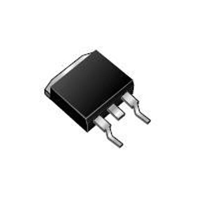
SOT-223 package:
Features: The SOT-223 package is larger than the SOT-89 package and has four leads. It offers improved thermal characteristics.
Examples: LM7805, LM317T
Applications: Linear voltage regulators, power management, battery charging circuits.
SOT-363 package:
Features: The SOT-363 package is very small and has six leads for electrical connections. It is commonly used for integrated circuits and small-signal transistors.
Examples: BC847, 2N7002
Applications: RF amplifiers, signal switching, small-signal applications.
In addition to TO and SOT packages, there are several other types of transistor packages commonly used in the electronics industry. Here are some of the notable ones:

QFP (Quad Flat Package): A square or rectangular package with leads on all four sides. Suitable for integrated circuits (ICs) with a large number of pins.
BGA (Ball Grid Array): A package with an array of solder balls on the bottom surface for electrical connections. It offers high pin density and is commonly used for microprocessors and high-performance ICs.
PLCC (Plastic Leaded Chip Carrier): A square or rectangular package with leads on all four sides, typically used for ICs.
QFN (Quad Flat No-Lead): A square or rectangular package with no leads extending from the sides. The electrical connections are made through pads on the bottom surface.
SON (Small Outline No-Lead): Similar to QFN, but with a smaller footprint.
Future trends in transistor packaging are driven by the need for higher performance, miniaturization, increased functionality, and improved thermal management. Here are some key trends to watch for:
Miniaturization: Transistors will continue to become smaller and more compact, enabling higher integration density and smaller electronic devices.
Advanced materials: New materials with improved thermal conductivity and electrical properties will be developed to enhance heat dissipation and overall performance.
3D packaging: Three-dimensional packaging techniques, such as chip stacking and package-on-package (PoP), will be increasingly utilized to increase integration capabilities and optimize space utilization.

System-in-Package (SiP): SiP technology combines multiple components, including transistors, into a single package, enabling higher functionality and reducing the overall size of the system.
Embedded die packaging: Transistors can be directly embedded within the substrate or PCB, reducing the size and complexity of the package and improving electrical performance.
Fan-out packaging: Fan-out packaging technologies allow for increased I/O density and improved signal performance by redistributing the transistor's connections beyond the chip area.
Wafer-level packaging (WLP): WLP eliminates the need for individual packaging of each transistor, leading to higher yield, improved electrical performance, and reduced cost.
Advanced thermal management: Enhanced thermal management techniques, such as microfluidic cooling and advanced heat sink designs, will be employed to address the challenges of dissipating heat from high-power transistors.
Heterogeneous integration: Different transistor technologies, such as CMOS, MEMS, and optoelectronics, will be integrated within a single package, enabling diverse functionalities and improved system performance.
Environmental considerations: Packaging solutions will focus on sustainability, incorporating eco-friendly materials and designs that minimize waste and facilitate recycling.
These trends reflect the ongoing drive for smaller, faster, and more efficient electronic devices. The future of transistor packaging lies in pushing the boundaries of integration, performance, and thermal management to meet the demands of emerging technologies and applications.
In conclusion, transistor packages play a crucial role in the successful implementation of electronic circuits, offering protection, convenience, and improved performance. By understanding the different types of transistor packages, their characteristics, and applications, you can make informed decisions in selecting the appropriate package for your project.
Stay updated with the latest advancements in transistor packaging technology, explore datasheets and application notes, and leverage the benefits of these packages to enhance the performance and durability of your electronic designs.
Hot News