The S8050 is an NPN epitaxial silicon transistor with low voltage and high current capability that is a highlight for push-pull amplification and general purpose switching applications.

The S8050 transistor consists of three layers, with one P-doped semiconductor layer encapsulated between two other N-doped layers, the P-doped layer representing the base terminal, and the other two layers representing the emitter and collector, respectively.
The S8050 triode has two PN junctions: a forward-biased emitter-base junction and a reverse-biased collector-base junction.
It is important to note that the S8050 transistor must be operated in forward bias mode for better performance. If the transistor is not forward biased, there will be no collector current no matter how much voltage is applied to the base terminal.
When a voltage is applied at the base terminal, amplification is a simple way for the transistor to absorb a small current that is then used to control a large current at the other terminals.
In the S8050 NPN transistor, both terminals, emitter and collector, are reverse biased when the base is grounded, and they are closed (forward biased) when a signal is supplied to the base pin.
The S8050 triode has a maximum gain value of 300. This value will determine the amplification capability and will be used if the amplification is very high.
However, the gain value for the collector current will be 110 and the maximum current supply across the collector terminals is 700mA, so we cannot control different loads by passing more than 700mA through this transistor. Once the current supply is supplied to the base pin, which must be limited to 5mA, the transistor can be biased.
Once the transistor is fully biased, it allows up to 700mA of current to be supplied through the emitter and collector terminals, so this phase is called the saturation region. 20V and 30V are typical voltages used on VCE or VCB, respectively.
Once the current source is removed from the base terminal of the transistor, it will be turned off, so this stage is called the cutoff region.

In the S8050 NPN transistor, electrons are the primary charge carriers, unlike the PNP transistor where holes are the primary charge carriers
The base is corrected with respect to the emitter, and the voltage on the collector must also be corrected with respect to the base.
Two current gain factors: common emitter current gain and common base current gain play a crucial role in determining the characteristics of the transistor.
The common emitter current gain is the ratio between the collector current and the base current, which is called beta and is expressed as β. It usually ranges from 20 to 1000, but the standard value is taken as 200.
Similarly, the common-base current gain is the ratio between the collector current and the emitter current, which is called alpha and is denoted by α. Its value is mainly between 0.95 and 0.99, but most of the time its value is taken as 1.
You may like: How Many Transistors in a CPU

Emitter: emitter, current flows through the emitter
Base: the base, controls the bias of the transistor
Collector: collector, current flows through the collector
Low voltage, high current NPN transistor
Small signal transistor
Maximum power:2 watts
Maximum DC current gain (hFE) is 400
Continuous Collector Current (IC) of 700 mA
Base-emitter voltage (VBE) is 5V
Collector-emitter voltage (VCE) of 20V
Collector-base voltage (VCB) of 30V
High level for push-pull configuration doe class amplifier
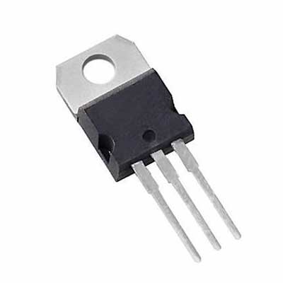
To-92 package available
More questions about S8050, check here: S8050 ST TO-92 Triodes
S8050 Complementary PNP Transistor: S8550
S8050 Replacement NPN Transistors: S9014, MPSA42, SS8050, BC547, 2N2369, 2N3055, 2N3904, 2N3906
S8050 equivalent transistors: 2N5830, S9013
As mentioned earlier, the S8050 features transistors typically used in push-pull configurations with Class B amplifiers. So let's discuss how to do this.
A push-pull amplifier, often referred to as a Class B amplifier, is a multi-stage amplifier typically used for audio amplification of loudspeakers. It is very simple in construction and requires only two identical complementary transistors. This means that we need an NPN transistor and its equivalent PNP transistor. A simple circuit diagram of a Class B amplifier using the S8050 is shown below.

Audio amplifier circuit
Class B amplifier
Push-pull transistors
Circuits requiring high gain
Low signal applications
For use in circuits requiring high levels
Used as a switch in different circuits.
It amplifies low gain signals to high gain
If designing a PCB or Perf board using this component, the following diagram in the S8050 transistor data sheet will help to understand its package type and dimensions.

1、S8050 transistor circuit symbol model diagram

2、S8050 transistor package size diagram

3、3D model of S8050 transistor

Hot News