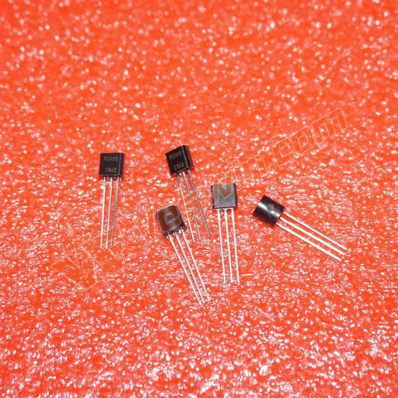
MOSFET transistors are widely used in analog and digital circuits, which are closely related to our life.
The advantages of MOSFET transistors are:
1. The driving circuit is relatively simple.
2. The drive current required for FETs is much smaller than that of BJTs, and can usually be driven directly by CMOS or open collector TTL circuits.
3. The switching speed of FETs is relatively fast, and they can operate at higher speeds due to the absence of charge storage effects.
4. In addition, FETs do not have a secondary breakdown failure mechanism, are more durable at higher temperatures, have a lower probability of thermal breakdown, and provide better performance over a wider temperature range. Field effects have been widely used in consumer electronics, industrial products, electromechanical devices, smart phones and other portable digital electronics.
In the future, mosfet transistors will still dominate. Mosfet transistors will remain a device that many engineers new to the field will be exposed to. Next, we will discuss some of the basics of FETs from the ground up, including the selection of key constants, introduction, system and thermal considerations, etc.
There are two types of FETs: N-channel and P-channel is the decision to use N-channel or P-channel MOS transistors. In a typical power supply application, the metal oxide semiconductor transistor is configured as a low-voltage side switch when the metal oxide semiconductor transistor is grounded and the load is connected to the supply voltage.
In low-voltage side switching, N-channel MOS transistors should be used considering the voltage required to turn off or on the device. When the metal oxide semiconductor transistor is connected to the bus and the load is grounded, it should be turned on and off on the high voltage side. P-channel MOS transistors are often used in this topology, also for voltage drive considerations.
Determine the required voltage rating or the voltage that the device can withstand. The higher the rated voltage, the higher the cost of the device. Based on practical experience, the rated voltage should be greater than the supply voltage or the bus voltage. This will provide sufficient protection against MOS tube failure.
In terms of selecting a metal oxide semiconductor transistor, it is necessary to determine the possible voltage between the drain and source, i.e. VDS. It is important to know that the voltage that the MOS tube can withstand will vary with temperature. We must test the voltage range over the entire operating temperature range.
The voltage rating must have enough margin to cover this range of variation to ensure that the circuit does not fail. Other safety factors to consider include voltage transients caused by switching electronics (such as motors or transformers).
The voltage ratings vary from application to application; generally 20 V for portable devices, 20 ~ 30 V for FPGA power supplies, and 450 ~ 600 V for 85 ~ 220 VAC applications. Kia Semiconductor designs MOS tubes with high voltage tolerance and wide application areas, which are favored by customers.
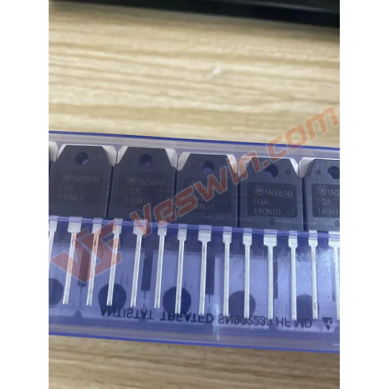
The rated current should be the current that the load can withstand under any circumstances. Similar to the voltage case, make sure the selected MOSFET transistor like 50N06L UTC TO-220 can withstand this rated current even if the system generates a peak current. The two current cases considered are continuous mode and pulse spikes.
In continuous conduction mode, the metal oxide semiconductor transistor is in a steady state and current flows continuously through the device. Pulse spikes are large surges (or spikes) that flow through the device. Once the current under these conditions is determined, it is straightforward to select only the device that can withstand that current.
Once the rated current is selected, the conduction loss must also be calculated. In fact, metal oxide semiconductor transistors are not ideal devices because of the power loss in the conductive process, which is called conduction loss. MOS transistors are like variable resistors in "conduction", determined by the RDS(ON) of the device, which varies significantly with temperature. The power consumption of the device can be calculated by Iload2×RDS(ON).
As the on-state resistance varies with temperature, the power loss also varies proportionally. The higher the voltage VGS applied to the MOS tube, the smaller the RDS(ON) will be; conversely the higher the RDS(ON) will be. Note that the RDS(ON) resistance will rise slightly with the current. Variations on the various electrical and pneumatic parameters of the RDS(ON) resistance can be found in the technical data sheets provided by the manufacturer.
Two different scenarios must be considered, namely the worst case and the real case. It is recommended that the worst-case calculation be used, as this result provides a greater margin of safety and can guarantee that the system will not fail. There are also some measurements in the MOS tube data sheet to note; the junction temperature of the device is equal to the ambient temperature plus the product of thermal resistance and power dissipation (junction temperature = ambient temperature + [thermal resistance × power dissipation]).
Based on this formula, the power consumption of the system can be solved for, defined as equal to I2×RDS(ON). We calculated the RDS(ON) at different temperatures based on the current of the device. In addition, the board and its MOS tubes should be well dissipated.
Avalanche breakdown is when the reverse voltage on a semiconductor device exceeds the value, creating a strong electric field that increases the current in the device. The increase in chip size will increase the avalanche resistance and ultimately improve the robustness of the device. Therefore, choosing a larger package can effectively prevent avalanches.
There are many parameters that affect the switching performance, but the most important are the gate/drain, gate/source, and drain/source capacitances. These capacitances contribute to the switching losses of the device as it is charged each time it is switched.
As a result, the switching speed of the metal oxide semiconductor transistor is reduced and the device efficiency is also reduced. In order to calculate the total losses of the device during switching, the losses during switching (Eon) and the losses during switching (Eoff) should be calculated.
The total power of the MOSFET switching can be expressed by the following equation: Psw= (Eon+Eoff)× switching frequency. The effect of gate charge (Qgd) on the switching performance.
Hot News