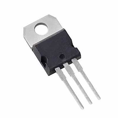
Transistors are broadly categorized into three types: bipolar, field effect and insulated gate bipolar.
Bipolar transistors (BJTs) are current drivers, while field effect transistors (FETs) and insulated gate bipolar transistors (IGBTs) are voltage drivers.
What is BJT
BJT stands for Bipolar Junction Transistor. It's a type of semiconductor device used in electronic circuits for amplification or switching purposes. BJTs come in two main types: NPN (negative-positive-negative) and PNP (positive-negative-positive), referring to the arrangement of the layers of semiconductor material.
They have three regions: the emitter, the base, and the collector. The flow of current in a BJT is controlled by the amount of current entering the base. When a small current flows into the base, it allows a much larger current to flow from the collector to the emitter (in the case of an NPN transistor).
BJTs are commonly used in amplifiers, voltage regulators, oscillators, and other electronic circuits due to their ability to control large currents with small ones and their fast response times.
NPN and PNP Construction
BJT Operation
Metal-oxide-semiconductor field effect transistors (MOSFETs) are the most popular transistors today.
There are two types of MOSFETs: N-channel and P-channel. the N-channel is widely used in AC/DC power supplies, DC/DC converters, inverter devices, etc., while the P-channel is used for load switching, high side switching, etc.
The differences between MOSFETs and BJTs are shown in the table below.
Aspect | BJT | MOSFET |
Input Impedance | Low | High |
Reverse Transfer Capacitance | Large | Small |
Safe Operating Area | Narrow | Wide |
Voltage Operation | Low (0.6V-0.7V for turn-on voltage) | Low gate power |
/ | - | Easy to Drive |
N-channel Mosfet
P-channel Mosfet
How Mosfet Works
(1) Apply a voltage between the drain and source where the drain is positive. (Drain-source voltage: VDS)
(2) Apply a voltage between the gate and source where the gate is positive. (Gate-source voltage: VGS)
(3) As a result, electrons are attracted to the p-type layer below the gate insulating film, and part of the p-type layer is transformed into an n-type region (the n-type region in the p-type layer is called the "inversion layer (channel)").
(4) When this inversion layer is completed, an n-layer path is formed from the drain to the source of the MOSFET.
(n+⇔n-⇔ inversion layer (n) ⇔ n+)
(5) Thus the MOSFET operates at low resistance and the drain current is determined by the applied VDS and load current
MOSFET Switching Applications
Since the MOSFET forms a channel based on the gate-source voltage, this voltage must be a certain or higher voltage. Once the trench is formed, the on-state continues and drain current continues to flow, so very little drive power is required. By releasing the charge built up in the gate and removing the trench, it transitions to the off state. (Driving voltage is higher than BJT, driving power is small)
Input capacitance (Ciss) = gate-drain and gate (Cgd) + gate-source capacitance (Cgs)
Reverse transfer capacitance (Crss) = gate-drain capacitance (Cgd)
Output capacitance (Coss) = gate-drain and drain ( Cgd) + source and gate-drain capacitance (Cds)
Rise time (tr): is the time for the drain-source voltage to change from 90 percent to 10 percent
Turn-on time (ton): the interval between the instant when the gate-source voltage rises to 10% and the instant when the drain-source voltage falls to 10%
Time to fall (tf): the time for the drain-source voltage to change from 10% to 90
Turn-off time (toff): the interval between the moment when the gate-source voltage drops to 90% and the moment when the drain-source voltage rises to 90%.
IGBT Overview
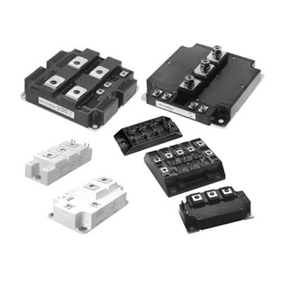
IGBT stands for Insulated Gate Bipolar Transistor. It's a type of semiconductor device that combines the high efficiency of a MOSFET (Metal-Oxide-Semiconductor Field-Effect Transistor) with the high current-handling capability of a bipolar transistor.
The IGBT consists of three main layers: a P-type substrate, an N-type drift region, and a P-type layer on top, forming an NPN sandwich structure. The gate of the IGBT is insulated from the main semiconductor material by a thin layer of oxide, similar to a MOSFET.
One key advantage of IGBTs is their ability to handle high voltages and high currents while having a fast switching speed. They are commonly used in various applications such as power supplies, motor control, renewable energy systems like wind and solar inverters, and in many other high-power electronic devices.
IGBTs are known for their efficiency in switching high power loads, making them an essential component in modern power electronics due to their ability to handle large currents and voltages efficiently with relatively low power loss.
Internal equivalent circuit of an IGBT
An IGBT is a device suitable for high-current control that has a voltage-driven MOSFET in the front stage and a transistor in the back stage that permits high-current flow.
An insulated gate bipolar transistor (IGBT) is a device that turns on and off the power between the collector and emitter by controlling the voltage between the gate and emitter in the same way as a MOSFET.IGBTs are better suited for controlling high voltages and large currents than MOSFETs.
BJT (Bipolar Junction Transistor), MOSFET (Metal-Oxide-Semiconductor Field-Effect Transistor), and IGBT (Insulated Gate Bipolar Transistor) are all types of semiconductor devices used in electronic circuits, each with its own characteristics and applications.
Here's a comparison:
Feature | BJT | MOSFET | IGBT |
Operation | Bipolar Junction Transistor | Metal-Oxide-Semiconductor Field-Effect | Insulated Gate Bipolar Transistor |
Control Mechanism | Current controlled | Voltage controlled | Voltage controlled, combines BJT & MOSFET |
Power Handling | Low to moderate power | Low to high power | Moderate to high power |
Conduction Losses | Relatively higher | Lower than BJT, higher than IGBT | Lower than BJT, similar to MOSFET |
Switching Speed | Faster than IGBT, slower than MOSFET | Faster | Slower than MOSFET, faster than BJT |
Applications | Amplifiers, low-power circuits | Digital circuits, high-frequency apps | Motor drives, power inverters, high-power apps |
Input Impedance | Moderate | High | Moderate |
Q: Which transistor type has the fastest switching speed?
A: MOSFETs generally have the fastest switching speeds among the three due to their high input impedance and low capacitance.
Q: Which transistor type is most suitable for high-power applications?
A: IGBTs are specifically designed for high-power applications due to their combination of high input impedance and low on-state voltage drop, which minimizes conduction losses in high-power scenarios.
Q: What are the major factors to consider when choosing between BJT, MOSFET, and IGBT?
A: Considerations include power requirements, switching speeds, voltage ratings, current-handling capacity, and efficiency demands. BJTs are suitable for lower power levels, MOSFETs excel in high-speed switching, and IGBTs shine in high-power applications.
Hot News
