LIN (Local Interconnect Network) is a low-cost network. Its initial development purpose is to make up for the shortcomings, which are mainly used in some occasions where the communication rate is not high. The use of LIN as the auxiliary network or sub-network of the CAN bus can solve many problems caused by excessive wires in the car.
In addition to a simple LIN node, two chips are needed, namely a LIN interface chip and a 5V regulator. The company's chips are single-wire devices dedicated to LIN. The device is very low, can control the external voltage regulator, safety meets the LIN specification, and has strong anti-interference ability. It is a high-performance analog device suitable for automobiles with relatively complex working environments. The main features of MC33399 are as follows:
· The communication rate range is 1 ~ 20kb / s;
· Rated working voltage: 8V ~ 18V, normal voltage: 7V ~ 27V;
· Reactive node does not affect the bus status;
· There are two working modes of normal and sleep, the static in sleep mode is only 20μA;
LIN bus wake-up, command wake-up and external high-voltage switch input wake-up;
Interface with MCU through compatible I / O pins;
· With external voltage regulator control function;
· Built-in pull-up;
The ESD voltage of the LIN pin can reach 4kV;
· Good electromagnetic compatibility;
· Working temperature range is -40 ℃ ~ 125 ℃.
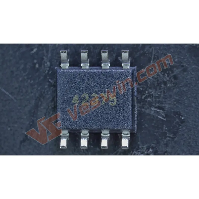
MC33399 adopts SO8 type patch type. Figure 1 shows the pin arrangement, and the functional description of each pin is listed in Table 1.

Figure 1 MC33399 pin arrangement
Table 1 Pin functions of MC33399
Pin number Pin name Function
1 RX receive data output
2 EN enable terminal
3 Wake terminal, used to wake the chip from sleep
4 TX transmit data input
5 GND Ground
6 LIN LIN bus interface
7 Vsup power supply
8 INH External regulator control terminal
The internal structure of MC33399 is shown in Figure 2. Now its main working principle is introduced as follows:

Figure 2 MC33399 internal structure block diagram
3.1 Main functions
The working mode of MC33399 is controlled by the enable terminal EN. When EN is 1, it is in a normal working state. At this time, the two transmission paths from the TX pin to the LIN bus and from the LIN bus to the RX pin are activated. When EN is 0, the chip enters sleep or mode, at this time the two transmission paths are prohibited. In sleep mode, the LIN pin can be maintained at high level Vsup through the and upper current source, and the quiescent current (typical value is 20μA) is provided by the power supply to the chip through the Vsup pin.
The LIN pin of MC33399 is used to complete the single bus transceiver function. The TX pin is used to control the output state of the LIN pin. During operation, the state of the two pins is always consistent. The RX pin can be used to display the status of the LIN bus. When the LIN bus is high (recessive), RX is high; otherwise, when the LIN bus is low (dominant), RX is low. The RX output is a typical CMOS push-pull output structure.
Due to its specific internal structure, there will be no reverse current from the LIN bus into the chip when the local drift or power connection fails. MC33399 allows Wake pin to input high voltage to wake up, and can also wake up from two transitions of Wake pin from high to low or from low to high. When the chip enters the sleep state, the chip will record the current state of the Wake pin. When the circuit detects the opposite state of the Wake terminal, it is considered that a wake-up event has occurred. In addition, the chip also has built-in noise, which can suppress the high-frequency noise interference of the bus and prevent false wake-up.
3.2 Wake up from sleep
MC33399 can wake up from sleep mode in the following three ways:
(1) LIN bus wake up
Any node on the bus can send a "wake-up frame" to change the state of the LIN pin from recessive to dominant to wake up the chip. When waking up, the MC33399 is in "waiting mode" and the INH pin is set high to activate the external regulator. After that, the MCU powers up and sets the EN pin to a high level, so that the chip enters the "normal mode" from the "waiting mode".
(2) Internal node activation and wake-up
When the MCU in the local node issues an instruction to set the EN pin high, the chip will also enter the "normal mode".
(3) Wake up via Wake pin
By setting a switch outside the MC33399 chip, the Wake pin input high voltage wakes up.
This circuit uses the wake-up mode of the Wake pin input switch, in which the 5V external voltage regulator is controllable. The EN pin is directly connected to the I / O port of the MCM and is used to select the working state of the MC33399. The communication receiving pin RX and the sending pin TX are respectively connected to the serial communication interface (SCI) of the MCU to complete the communication function. The INH pin is directly connected to the control terminal of the external voltage regulator. When the circuit is working normally, the INH pin outputs a high level, the external voltage regulator is activated, and the normal output 5V voltage supplies power to the MCU; and when the chip enters sleep mode , INH pin output low level to disable the external voltage regulator, MCU power off. In addition, the INH pin can also be connected to the IRQ or XIRQ pin of the MCU via a transistor to generate an interrupt. At this time, the external voltage regulator should be uncontrollable.
Because the internal LIN pin and Vsup pin are integrated with pull-up resistors and series, the bus slave node does not require external pull-up components. However, for the master node, a 1kΩ pull-up resistor must be added externally, and a diode must be connected in series to prevent the MC33399 from being powered up through the bus when the battery is powered down.
An external switch through the Wake pin can input high voltage to the Wake pin to call the MC33399 from sleep mode. When the input voltage of the Wake pin exceeds 14V, in order to prevent the input current from being too large, a series resistor must be connected to limit the instantaneous (resistance value is generally 33kΩ). At the same time, it must be noted that the Wake pin must not be left floating. If this pin is not used, it must be grounded to prevent false wake-up.
An external switch through the Wake pin can input high voltage to the Wake pin to call the MC33399 from sleep mode. When the input voltage of the Wake pin exceeds 14V, in order to prevent the input current from being too large, a series resistor must be connected to limit the instantaneous pulse current (the resistance value is generally 33kΩ). At the same time, it must be noted that the Wake pin must not be left floating. If this pin is not used, it must be grounded to prevent false wake-up.
MC33399 circuit is widely used in automobile body control system with its perfect performance. The 8-pin circuit LT1121 can be used as the external regulator used with this circuit. In fact, these two chips will be replaced by Freescale's new System Basis Chip (SBC).
Hot News