What is the ultimate significance of FPGAs in the data age? In terms of characteristics, compared to frozen ASICs that execute algorithms outside the core, FPGAs with programmable cores have strong flexibility and adaptability; in terms of functionality, it is Moore’s Law The coprocessors and bridge devices that are critical to slow down.
In the context of heterogeneous computing, FPGAs are increasingly pursuing small size, low power consumption and high performance. This is the inherent characteristics of FPGAs. It can be said that FPGAs are the most suitable products in the data age at this stage. In the pursuit of extreme performance, in addition to increasing the number of I/Os, some manufacturers even put ASICs into FPGAs in pursuit of flexibility and adaptability.
Lattice (Lattice Semiconductor) uses the 28nm FD-SOI (depletion-mode silicon-on-insulator) process to balance the performance and power consumption of FPGAs, so that small FPGAs have both "high performance" and "low power consumption". Kind of characteristics. Technically speaking, it is mainly because FD-SOI can control the voltage in this part of the substrate, so the feedback bias (Back Bias) is controllable. In this respect, low power consumption and high performance settings can be switched freely. .
On the other hand, traditional FPGA products using SRAM manufacturing process are susceptible to radiation interference, while 28nm FD-SOI has a thinner oxide layer, so the reduction of critical areas reduces the soft error rate (SEU). At the same time, compared with the bulk CMOS process, the leakage of 28nm FD-SOI is also reduced by 50%.
Using this 28nm FD-SOI process, Lattice released the Lattice Nexus™ technology platform last year to produce multiple series of products, and at the same time also released its first product, CrossLink-NX. Previously, 21ic China Electronics Network has also focused on explaining this process FPGA.
Just six months after the first product came out, Lattice recently announced the release of the second-generation product of this platform-Certus™-NX. This new product has outstanding parameters and performance of the same type of product, and has higher 21ic China Electronics Network reporter was invited to participate in this conference.
Of course, it should be noted that Lattice has been focusing on the mid-range market, and the main scope is still low-power small FPGAs. The products are mainly focused on functionality and cost-effectiveness, and this product is also the case.
From the overall architecture point of view, because both Certus-NX and CrossLink-NX use 28nm FD-SOI process, they are very similar in characteristics, can switch between low power consumption and high performance modes, embedded embedded flash memory, and configured The unique DSP module performs multiplication and addition.
In addition, the logic unit is also 17-40K. In terms of fast startup, both use Lattice's consistent embedded flash memory, which greatly reduces the wake-up time and achieves a seamless visual experience.
From the perspective of differences, the two products have two key points of distinction:
1. Certus-NX removes the hard-core MIPI D-PHY
According to the introduction of Jeffery Pu, director of Lattice’s on-site technical support, this is mainly an optimization that takes into account the number of I/O requirements in the sub-molecule market. After removing the hard-core MIPI D-PHY, the I per square millimeter The number of /O has increased significantly.
The reporter compared the parameters of the two products. The minimum size of the two products is 6 x 6 mm (121 csfBGA). The number of I/Os of CrossLink-NX is 72, while the number of I/Os of Certus-NX is 82, which is equivalent to a 13% increase in the number of I/Os per square millimeter.
In terms of applications, MIPI interfaces are mostly related to cameras and sensors. The previous generation of markets aimed at embedded vision in the consumer market, while this product focuses more on network edge applications to add processing and interconnection functions. These applications Generally speaking, PCle and Gigabit Ethernet are emphasized. Because of this, this generation of products takes the ultimate cost performance and ultimate power consumption performance, turning hard cores into performance for different application markets.
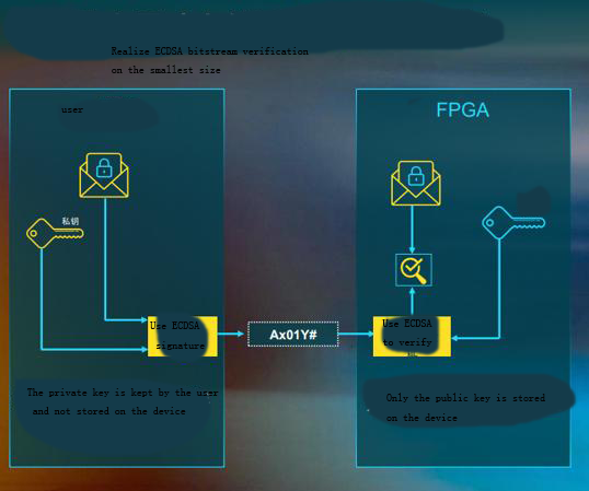
2. Certus-NX adds the safety certification ECDSA bit stream verification
Jeffery Pu told reporters that he was inspired by the previous generations of products, including the XO3D products previously launched by Lattice, which have PFR functions and complex certifications. Borrowing these concepts and putting them into new products, this is very different from the previous generation products. Obvious gap.
Technically speaking, the English full name of ECDSA is Elliptic Curve Digital Signature Algorithm. The main principle is to create a digital signature of data. Unlike AES (Advanced Encryption Standard), ECDSA does not encrypt data or prevent data access. Of course, this FPGA also supports strong AES-256 bit stream encryption.
From the market point of view, users who need to work hard in embedded vision can choose CrossLink-NX with MIPI interface, and those who need to focus on industry and communication to add processing and interconnection can choose the more powerful Certus-NX .
With the support of 28nm FD-SOI process and Lattice's consistent low-power FPGA experience, the new product stands out among similar competitors. It should be noted that Lattice has repeatedly emphasized that its focus is on consumer-grade low-power FPGAs. The market needs both manufacturers pursuing cutting-edge market products and FPGA manufacturers focusing on small-size products. The specific comparison is as follows:
1. 3 times smaller size, 2 times I/O quantity, 70% I/O rate increase
Certus-NX is only 6 x 6 mm in the smallest size. The 50K logic unit products of company A, which are the closest in terms of I/O number and speed, have reached the size of 10 x 10 mm, while the 77K logic of company B The unit product has reached 11 x 11 mm, which is a three-fold difference.
In terms of the number of I/Os, on the one hand, the 28 nm FD-SOI process is supported. On the other hand, after all, this generation of products has cut off the MIPI hard core, and the increase in number is quite obvious. Of course, compared with traditional craft products, the rate has also increased by 70% under the blessing of 28 nm FD-SOI technology.
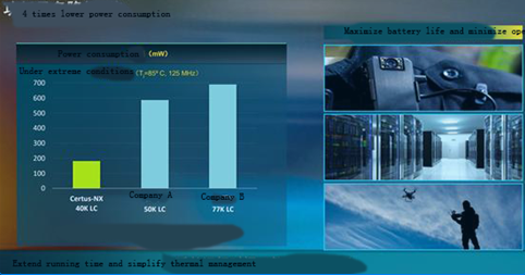
2. 4 times lower power consumption
Lattice's long-standing advantage has been low power consumption. From the point of view of parameters, compared with company B's 77K logic unit products under extreme conditions, it is reduced by up to 4 times.
On the other hand, low power consumption means lower heat generation, and in this regard, the battery has a maximized lifespan. This means that electricity costs, heat dissipation costs, and battery replacement costs are all reduced.
3. 12 times configuration speed
Configuration speed has always been Lattice's strengths, and this feature has been added since CrossLink-Plus. The main principle is to embed embedded flash memory in the product to speed up the startup speed. This generation of products still follows the 3ms I/O configuration time of the previous generation.
Jeffery Pu told reporters that traditional FPGAs generally add SPI Flash, and the startup speed depends on the speed of SPI. In the early years, traditional FPGAs were able to run at 50Mbps, which is very good. Nowadays, the new SPI Flash can basically reach 130Mbps, but it is still not able to achieve the effect of seconds.
Certus-NX mainly uses QSPI. Compared with single-channel SPI, the data loading speed of four channels will be significantly improved. However, it should be noted that this requires the FPGA to have a corresponding design to support rapid configuration.
In many cases, in a security-oriented system, a delay in the startup time will bring certain risks. The seamless startup display not only brings a better user experience, but also adds a touch to safety.
4. 100 times to reduce the soft error rate (SER)
According to the data released by Certus-NX, the SER under 40K logic unit reached 19.34, which is more than 100 times lower than the 50K logic unit product of Company A. This is attributed to the inclusiveness of the 28nm FD-SOI process, which has a thinner oxide layer, which reduces the critical area and thereby reduces the soft error rate (SER).
Of course, not only the soft error rate is an indicator, this process also has anti-interference, and the leakage is also reduced by 50%.
In addition to the latest FPGA, Lattice also released the latest software solution called Lattice Propel in the first half of the year. It is understood that the Lattice Propel development tool contains two major features: IP integration tool Lattice Propel Builder, and software development tool Lattice Propel SDK.
Propel means driving and advancing, and these two development tools have effectively further promoted the automation of FPGA development. Lattice Propel Builder allows FPGA developers to design in the form of dragging IP blocks, and can also automatically generate code online; Lattice Propel SDK has software suite construction, compilation, analysis and debugging applications, and software libraries Provide support with the development board, allowing software developers to design software before the hardware is ready, speeding up the time to market.
It is worth mentioning that Lattice Propel supports RISC-V IP. As we all know, RISC-V is extremely important in embedded applications. Through the latest FPGA development environment, the industry will usher in a new development pattern.
Of course, related tools and IPs based on Certus-NX are also available for download, and developers will have a better development experience. Currently, Certus-NX samples have been sent to multiple customers, and development boards are available for ordering.
At the end of the press conference, Jeffery Pu revealed that the third generation of the 28nm FD-SOI Nexus technology platform will be announced in the second half of this year, and there are many related plans. The low-power FPGA market will have more surprises in the second half of the year. look forward to.
Hot News
